MitySOM-A5 / A5E Thermal & Power Performance
This page consolidates two related testing efforts on the MitySOM-A5 / A5E (Agilex 5) product line:
- DevKit Heat Dissipation — system-level power draw and case/die temperature measured on the MitySOM-A5 DevKit across different heatsink and airflow configurations (work in progress).
- FPGA Core-Rail Power & Thermal Characterization — controlled, repeatable core-rail power and die-temperature measurements using a purpose-built synthetic FPGA load ("heater" IP), independent of any customer application.
Together these give customers both a real-world system power/thermal reference (Part 1) and a way to reason about worst-case core-rail power scaling with FPGA utilization and clock frequency (Part 2).
Part 1: DevKit Heat Dissipation
THIS SECTION IS A WORK IN PROGRESS
This section provides some basic information about the thermal performance of the MitySOM-A5 (revision 1, with engineering silicon). It captures some basic scenarios using the MitySOM-A5 DevKit, and documents various power draw and thermal measurements made in the test.
Summary
| Scen | Heatsink | Airflow | SOM Volt | SOM Cur | SOM Pwr | Amb. Temp | A5 Temp | A5 Rise | Core Cur (1) | DevKit Volt | DevKit Cur | DevKit Pow | Notes |
|---|---|---|---|---|---|---|---|---|---|---|---|---|---|
| 2 | None | N | +12 V | 606 mA | 7.26 W | 24 C | 72 C | 48 C | 11.5 A | 12 v | 0.74 A | 8.89 W | 20 mins after power up |
| 2 | None | Y | +12 V | 24 C | 43 C | 19 C | 20 mins after power up | ||||||
| 2 | Passive 25x25 | N | +12 V | 603 mA | 7.21 W | 24 C | 67 C | 43 C | 11.8 A | 12 | 0.72 A | 8.65 W | 20 mins after power up |
| 2 | Passive 25x25 Spreadfin | N | +12 V | 571 mA | 6.75 W | 24 C | 65 C | 41 C | N/A | N/A | N/A | N/A | 20 mins after power up |
| 2 | Passive 25x25 Spreadfin | Y | +12 V | 516 mA | 6.17 W | 24 C | 37.5 C | 13.5 C | N/A | N/A | N/A | N/A | 20 mins after power up |
| 2 | Passive 25x25 | Y | +12 V | 539 mA | 6.45 W | 24 C | 39 C | 15 C | 10 A | 12 | 0.66 | 7.92 W | 20 mins after power up |
| 2 | Active 23x23 | Y | +12 V | 540 mA | 6.47 W | 25 C | 47 C | 23 C | 10.5 A | 12 V | 0.7 A | 8.4 W | 12 hrs after power up |
| 2 | Active 23x23 | Y | +5 V (2) | 730 mA | 3.56 W | 24 C | 39 C | 15 C | 9.0 A | 12 V | 0.16 A | 1.9 W | 20 mins after power up |
Additional Notes
- The PM Bus current readout from the power chips appears to have a bias or is impacted by the LDO voltage.
- To power the SOM at +5V, JP1 resistor was removed and a wire tacked into VIN_MONITOR net on devkit board. UVLO on input switch limits minimum voltage to about 10 V because of PCIe interface. There is a +5V LDO in the core supplies that appears to account for about 1.9 W at +12V input. The DevKit power now represents power not consumed by the SOM.
- The 'Y' in the 'Airflow' column for the active heatsinks is for the fan on the heatsink, no additional airflow was provided via a desktop fan.
- The 'SOM Pwr' readings come from the on-module power sensor, the 'DevKit Pow' readings come from an external power supply used to supply power to the DevKit.
Thermal options
| No Heatsink, Passive Airflow | Passive 25x25x8mm heatsink, Passive Airflow |
|---|---|
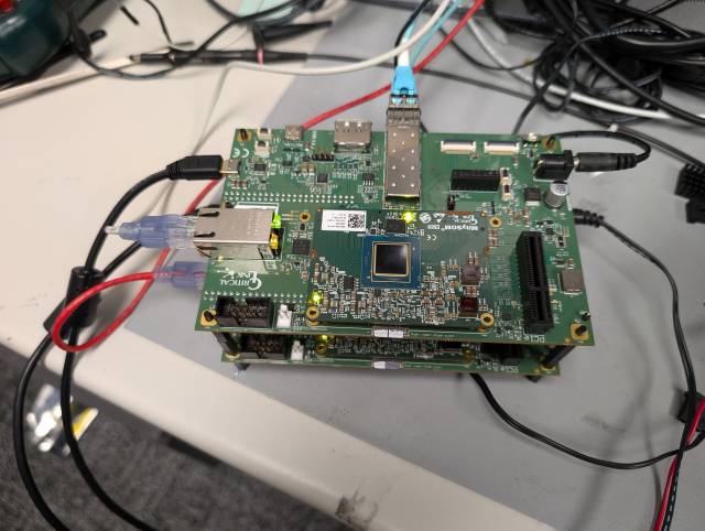 |
 |
| Passive 23x23x14.5mm spreadfin heatsink, Passive Airflow | Active 23x23 heatsink with integrated fan |
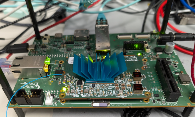 |
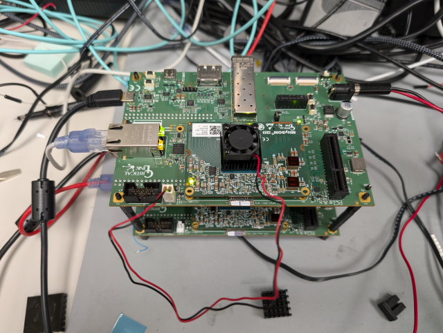 |
Configurations tested without a corresponding photo: No Heatsink w/ Forced Airflow; Passive 25x25x8mm heatsink w/ Forced Airflow.
Load Scenarios
Scenario 1: Booted to Uboot
Scenario 2: Boot to linux
In this scenario, the base_project is loaded into the FPGA bitstream and the processor allowed to boot to linux and essentially run IDLE while connected to the network. The board was allowed to run for at least 20 minutes before checking the temperature.
Scenario 3: QSFP+ Packet Test
Part 2: FPGA Core-Rail Power & Thermal Characterization (Heater IP)
This section summarizes thermal and power characterization testing performed on the MitySOM-A5E (Agilex 5) System-on-Module, covering FPGA core rail power and thermal behavior under controlled load conditions. It is intended to help customers understand the operating conditions this module has been tested under, how the data was collected, and how to interpret it for their own thermal and power budgeting.
Overview: FPGA core rail power & thermal testing
The Agilex 5 FPGA's internal core logic fabric draws power on a dedicated 0.8 V VCC core rail. How much power that rail draws — and how hot the die gets as a result — depends on how much of the FPGA fabric is used and at what clock frequency. To characterize this relationship under controlled, repeatable conditions, Critical Link developed a purpose-built test IP internally referred to as the "heater."
The heater is a synthetic FPGA logic block that can be built at a chosen size (occupying a target percentage of the device's logic resources — LUTs, DSP blocks, and block RAM) and driven at a controllable duty cycle via a software register (0–100%, similar to PWM). This provides a known, repeatable, adjustable load on the core rail, independent of any particular customer application — making it possible to directly measure how core power and die temperature scale with FPGA utilization, clock frequency, and cooling configuration.
Methodology
Equipment:
- LTC2945 power monitor IC on the SOM's 12 V input rail, used to measure input voltage, current, and power during load sweeps.
- On-die/on-package temperature sensors (
soc64hwmon) reporting four locations: SDM and three die corners (bottom-left, bottom-right, top-right). - Rigol MSO5354 oscilloscope, used separately to capture VCC_CORE rail ripple under load.
Procedure:
- The heater IP is built into an FPGA image at a chosen size (fraction of device logic resources used) and clock frequency, then loaded onto the target board.
- A software control script sweeps the heater's duty-cycle register from 0% to 100% in steps, holding briefly at each step, while logging SOM input power (via LTC2945) and, for thermal runs, die temperature.
- Because the Agilex 5 devices used here belong to a "Group A" (SmartVID) power delivery configuration, the 0.8 V core rail current cannot be read directly over I2C (the on-chip Secure Device Manager owns that bus). Core-rail current is therefore derived from the measured rise in 12 V SOM input power, divided by the 0.8 V rail voltage. This is a conservative upper-bound estimate of core dynamic current (it does not subtract DC-DC conversion losses), reported alongside the directly measured input power figures.
- Soak tests run the heater at a fixed duty cycle for an extended period (minutes) to observe whether die temperature reaches a stable plateau or continues to climb, under two cooling conditions: a heatsink with external forced-air cooling, and a heatsink alone with no forced air. A safety cutoff automatically disables the heater if any monitored die temperature exceeds 100°C (the Agilex 5's maximum rated junction temperature).
- Duty-cycle sweeps (heatsink-only) step the duty cycle upward and hold each level until the hottest die temperature stabilizes, to find the highest duty cycle sustainable without active cooling.
Data
1. Core-rail power vs. FPGA utilization and clock frequency (full duty / 100% load)
Measured on hardware, SOM 12 V input power via LTC2945. "ΔI_core" is the derived core-rail dynamic current estimate described in Methodology.
| FPGA utilization | Clock | Idle input power | Full-load input power | Δ Input power (heater) | Derived ΔI_core (0.8 V) |
|---|---|---|---|---|---|
| 53% ALM | 100 MHz | 6.82 W | 9.22 W | 2.40 W | 3.00 A |
| 53% ALM | 200 MHz | 7.14 W | 12.25 W | 5.11 W | 6.38 A |
| 53% ALM | 250 MHz | 7.26 W | 13.45 W | 6.19 W | 7.74 A |
| 73% ALM | 200 MHz | 7.29 W | 14.48 W | 7.19 W | 8.98 A |
| 78% ALM | 250 MHz | 7.67 W | 15.72 W | 8.05 W | 10.06 A |
| 78% ALM + 66% block RAM | 250 MHz | 7.77 W | 15.94 W | 8.17 W | 10.21 A |
| 77% ALM / 75% DSP / 79% RAM (larger device) | 200 MHz | 9.13 W | 20.59 W | 11.46 W | 14.32 A |
Note: the last row uses a larger Agilex 5 device (A5ED065 vs. A5ED043 for the other rows) with a balanced, high utilization across logic, DSP, and memory resources simultaneously — representing the highest core-rail load measured in this test campaign.
2. Duty-cycle sweep — power and temperature (heatsink only, no forced air)
Highest-utilization configuration tested (77%/75%/79% logic/DSP/RAM, 200 MHz), stepped in duty cycle with the hottest on-die sensor allowed to reach a stable plateau at each step before advancing.
| Duty cycle | Hottest die, steady-state | Input power |
|---|---|---|
| 40% | 77.1 °C | 14.3 W |
| 50% | 81.8 °C | 15.5 W |
| 60% | 87.1 °C | 16.8 W |
| 70% | 92.1 °C | 18.2 W |
The relationship between input power and steady-state die temperature was approximately linear over this range (roughly 3.8°C per additional watt, in this warm-soak test condition — see caveats below).
3. Soak test — sustained 100% duty cycle, fan vs. no forced air
Same configuration as above (highest-utilization build, ~20 W fabric load), run continuously at full duty cycle. Both runs used the same heatsink; only the presence of forced-air cooling differed.
| Cooling condition | Outcome | Hottest die reached | Input power | Time to reach limit |
|---|---|---|---|---|
| Heatsink + external fan | Stable — reached equilibrium at ~90 s, held for the full 10-minute test | ~56.4 °C | ~19.8–19.9 W | Did not reach cutoff |
| Heatsink only, no forced air | Automatic thermal cutoff triggered | 100.75 °C | Rose from 19.9 W to 21.7 W as temperature increased | 410 s (≈6 min 50 s) |
The automatic safety cutoff (set at the device's 100°C maximum junction temperature) engaged correctly and shut the load off, after which die temperature dropped rapidly.
4. Bench power consumption reference points
General bench-measured power figures for reference designs (not the heater load — these represent more typical application-level activity):
| Configuration | Measurement | Value |
|---|---|---|
| Holoscan design (MitySOM-STD + DevKit), idle, no cameras | Bench supply | 11.16 W |
| Holoscan design, 5 cameras streaming | Bench supply | 13.8 W |
| PCIe Gen4 x4 root-port design (Agilex 5, A5ED065) | FPGA core rail (fabric) | 2.305 A (~1.84 W) |
| PCIe Gen4 x4 root-port design | Total on-chip power | 6.51 W |
The PCIe reference design figure illustrates that a typical customer FPGA design (in this case, a PCIe root port) loads the core fabric far more lightly (~2.3 A) than the heater's maximum demonstrated load (~14.3 A) — the heater tests represent a stress-test upper bound, not typical operating power.
5. VCC_CORE rail ripple, no load vs. full heater load
Oscilloscope measurement on the core rail, MitySOM-STD:
| Measurement | No load | Full heater load (~20 W) |
|---|---|---|
| Average voltage | 835.4 mV | 829.1 mV |
| Peak-to-peak ripple | 31.4 mV | 48.4 mV |
| Min / Max excursion | 820.7 / 852.1 mV | 806.3 / 854.8 mV |
Under full heater load, the core rail's average voltage droops slightly (~6 mV) and ripple increases by roughly 50%, remaining within normal regulator operating margins.
Glossary & reference notes
- Duty cycle — in this context, the percentage of time the heater IP's internal logic is actively toggling within each PWM-style period. 100% duty cycle represents maximum sustained switching activity (and maximum power draw); 0% is idle.
- Core rail / VCC_CORE — the internal power supply rail (0.8 V nominal on the Agilex 5) that powers the FPGA's core logic fabric, separate from I/O and peripheral supply rails.
- Soak test — a test that holds a fixed load or condition constant for an extended period to observe whether temperature (or another parameter) reaches a stable equilibrium or continues to trend upward.
- Junction temperature (Tj) — the temperature of the semiconductor die itself, as distinct from the surrounding package, heatsink, or ambient air temperature. The Agilex 5 devices tested have a maximum rated Tj of 100°C.
- LTC2945 — a power monitor IC used to measure voltage, current, and power on the SOM's 12 V input supply during testing.
- ALM (Adaptive Logic Module) — the basic logic resource unit on Intel/Altera Agilex FPGAs; "% ALM" indicates what fraction of the device's total logic capacity a given FPGA build uses.
- SmartVID / "Group A" devices — an Agilex 5 power-delivery configuration where the core-rail voltage regulator's control bus is managed internally by the FPGA's Secure Device Manager, meaning core-rail current cannot be read directly from the Linux-accessible I2C bus (hence the input-power-based estimation method described above).
- Quartus Power Analyzer — Intel/Altera's FPGA design tool used to produce vectorless (estimated) power figures from a compiled design, useful for early estimates but generally lower than real measured power under actual switching activity.
Caveats & applicability
- No-forced-air results represent worst-case passive cooling, not necessarily a customer's actual thermal solution. Actual sustainable duty cycle/power in a customer enclosure will depend on that enclosure's airflow, ambient temperature, and heatsink design.
- The duty-cycle sweep steady-state temperatures (Data section 2) were measured on a warm-soaked board (following back-to-back full-load runs), meaning the starting/idle temperature was already elevated (~56°C hottest die) compared to a cold start (~33°C). The safe duty-cycle levels shown should be treated as a conservative floor, not the true ceiling — a system starting from a cold, properly ventilated state should sustain a higher duty cycle before reaching the same temperatures.
- Core-rail current figures for "Group A" Agilex 5 devices are derived estimates (from 12 V input power rise, divided by 0.8 V), not direct core-rail measurements, and represent a conservative upper bound. They are reported alongside directly measured input power so customers can see the underlying measurement.
- The heater IP represents a synthetic, worst-case stress load, not typical application power. Real customer FPGA designs (see the PCIe reference design in Data section 4) generally draw substantially less core-rail power than the heater's maximum demonstrated load.
- Test results are specific to the builds and devices indicated (device part number, logic utilization, and clock frequency are noted per row/section) — figures do not automatically generalize across different Agilex 5 device variants or build configurations.